
- Why FlashROM saving is confusing
- The 1 → 0 rule
- Run the writer from RAM
- The basic Flash command sequences
- Tested Z80 routines
- DQ7 / DQ5 status polling
- Flash sector geometry and ROM placement
- MSX pages, mapper banks and Flash sectors
- MegaFlashROM SCC+ SD
- Carnivore2
- ASCII16-X and openMSX
- Recommended save design
- Troubleshooting checklist
1. Why FlashROM saving is confusing
A Flash cartridge looks like ROM during normal execution, but compatible NOR Flash chips recognize special write sequences as commands. The CPU is still performing ordinary memory writes; it is the Flash chip that recognizes the address/value pattern and switches into program or erase mode.
The same basic AMD/JEDEC command set is used by the Flash chips found in ASCII16-X, MegaFlashROM SCC+ SD and Carnivore2. The complicated part is usually not the program byte command itself. The complications are mapper setup, sector geometry, cartridge write protection, and knowing what the Flash returns while an operation is still in progress.
2. The most important rule: Flash changes 1 → 0
An erased NOR Flash byte contains FFh. Programming can clear any of those 1 bits to 0. Programming cannot restore a cleared 0 bit back to 1. Restoring 0 → 1 requires erasing the entire sector containing the byte.
FFh → F0h → C0h → 00h    ; valid without erasing
FFh → F0h → F8h           ; invalid: some 0 bits would need to become 1
A useful software test before programming a byte is:
(old_value AND new_value) = new_valueIf that expression is true, the update requires only 1 → 0 transitions and can be programmed without erasing. If it is false, the containing sector must be erased first.
00h consumes all eight available 1-bits in that byte. After that, the byte cannot be changed to any other value until its sector is erased.
3. Execute Flash-writing code from RAM
Do not execute the program/erase routine from the FlashROM that is being placed into command/program/erase mode. Copy the writer into normal MSX RAM and call it there. A location such as C000h–E000h is convenient if it is available to the game.
This also avoids problems when the mapper banks being modified are the same banks from which code would otherwise be fetched.
4. Standard command sequences
Byte program
AAh → unlock address 1
55h → unlock address 2
A0h → unlock address 1
data → target Flash address
Sector erase
AAh → unlock address 1
55h → unlock address 2
80h → unlock address 1
AAh → unlock address 1
55h → unlock address 2
30h → any address inside the target sector
In the tested mapper arrangement below, those MSX-visible command locations are 4AAAh and 4555h. The target address must, of course, be in the Flash sector and bank you actually intend to modify.
5. Tested Z80 routines
The following routines are based on the code used and tested by Max Iwamoto with ASCII16-X, MegaFlashROM and Carnivore2, including the Illusion City ROM build.
; ------------------------------------------------------------
; FLASH PROGRAM
;
; HL = source in RAM
; DE = destination address in mapped Flash
; BC = number of bytes
;
; Return:
;   Cy = 0 success
;   Cy = 1 Flash operation failed
; ------------------------------------------------------------

_flash_program:
        LD      A,AAh           ; Unlock
        LD      (4AAAh),A
        LD      A,55h
        LD      (4555h),A
        LD      A,A0h           ; Byte-program command
        LD      (4AAAh),A

        LD      A,(HL)
        LD      (DE),A
        CALL    _check_flash_status
        RET     C               ; Error

        INC     HL
        INC     DE
        DEC     BC
        LD      A,B
        OR      C
        JR      NZ,_flash_program
        RET


; ------------------------------------------------------------
; FLASH SECTOR ERASE
;
; Example below targets a sector visible at 8000h.
;
; BC = 8030h is deliberately chosen because:
;   BC itself is an address inside the target sector
;   B = 80h = erase-setup command
;   C = 30h = sector-erase confirmation command
;
; Return:
;   Cy = 0 success
;   Cy = 1 Flash operation failed
; ------------------------------------------------------------

_flash_erase:
        LD      HL,4AAAh
        LD      DE,4555h
        LD      BC,8030h        ; Address inside target sector
                                ; B=80h, C=30h

        LD      (HL),L          ; AAh -> 4AAAh
        LD      A,E             ; A = 55h
        LD      (DE),A          ; 55h -> 4555h
        LD      (HL),B          ; 80h erase setup

        LD      (HL),L          ; AAh again
        LD      (DE),A          ; 55h again

        LD      A,C             ; 30h
        LD      (BC),A          ; Sector erase confirm

        LD      A,FFh           ; Expected result after erase
        LD      D,B
        LD      E,C             ; DE = address being polled

; ------------------------------------------------------------
; FLASH STATUS
;
; A  = expected final value
; DE = Flash address to poll
;
; Cy = 0 success
; Cy = 1 failure
; ------------------------------------------------------------

_check_flash_status:
        PUSH    BC
        LD      C,A

.loop:
        LD      A,(DE)          ; Flash status while busy
        XOR     C
        JP      P,.exit         ; DQ7 matches expected: finished

        XOR     C               ; Restore actual status value
        AND     20h             ; DQ5: exceeded timing limits?
        JR      Z,.loop

        ; DQ5 became 1. Re-read DQ7 once because the operation
        ; may have finished at about the same instant.
        LD      A,(DE)
        XOR     C
        JP      P,.exit

        SCF                     ; Cy=1: operation failed
        LD      A,F0h
        LD      (DE),A          ; Reset Flash to read-array mode

.exit:
        POP     BC
        RET
Why BC=8030h?
This is a code-size trick, not a Flash requirement. 8030h is simply an address inside the target sector, but its high and low bytes are also exactly the two erase command values needed later:
B = 80h     ; erase setup
C = 30h     ; sector erase confirm
The final 30h does not need to be written to the first byte of the sector. Writing it anywhere inside the target sector identifies which sector the Flash should erase.
6. What DQ7 and DQ5 actually mean
While a program or erase operation is active, a read from the target address is not necessarily the normal stored ROM byte. The Flash temporarily returns operation status.
| Bit | Meaning while an embedded operation is active |
|---|---|
| DQ7 | Returns the inverse of the expected DQ7 value while busy. When DQ7 matches the expected final value, the operation has completed. |
| DQ6 | Toggles between successive reads while an operation is active. Some Flash routines use this as an alternate polling method. |
| DQ5 | “Exceeded timing limits.” Indicates that the Flash could not complete the requested operation normally. |
The routine uses:
LD      A,(DE)
XOR     C
JP      P,.exit
After XOR C, bit 7 is zero when DQ7 equals the expected DQ7. JP P therefore detects successful completion without needing a separate mask and compare.
If DQ7 still does not match, the routine restores the original status byte and checks DQ5:
XOR     C
AND     20h
JR      Z,.loop
If DQ5 becomes set, the routine reads DQ7 one more time. That second check matters because completion and the observation of DQ5 can happen at nearly the same time. If DQ7 still does not match, the routine returns carry set and writes F0h to return the Flash to normal read-array mode.
FFh during a supposed programming operation, do not assume that the polling routine is wrong. It often means the command sequence was never accepted: the wrong mapper is active, the wrong bank is mapped, the command addresses do not reach the intended physical Flash locations, or write access is disabled.
7. Flash sector geometry: bottom-boot, top-boot and uniform
Flash documentation uses the word sector or erase block for the smallest area that can be erased independently. These are physical regions inside the Flash chip. They are not MSX 16 KB pages and they are not mapper banks. To avoid three different meanings for “page,” this article calls them Flash sectors.
The three layouts you are likely to encounter
| Physical layout | Small sectors | Rest of the chip | Practical consequence |
|---|---|---|---|
| Bottom-boot | The lowest physical 64 KB is split into eight 8 KB sectors. | Ordinary 64 KB sectors. | Useful for firmware components, but software must not assume every sector is 64 KB at the bottom of the chip. |
| Top-boot | The highest physical 64 KB is split into eight 8 KB sectors. | Ordinary 64 KB sectors. | The irregular sectors are at the opposite end of the chip. |
| Uniform | None. | Every erase sector is normally 64 KB. | The simplest layout, but software should still verify the actual device when it depends on exact geometry. |
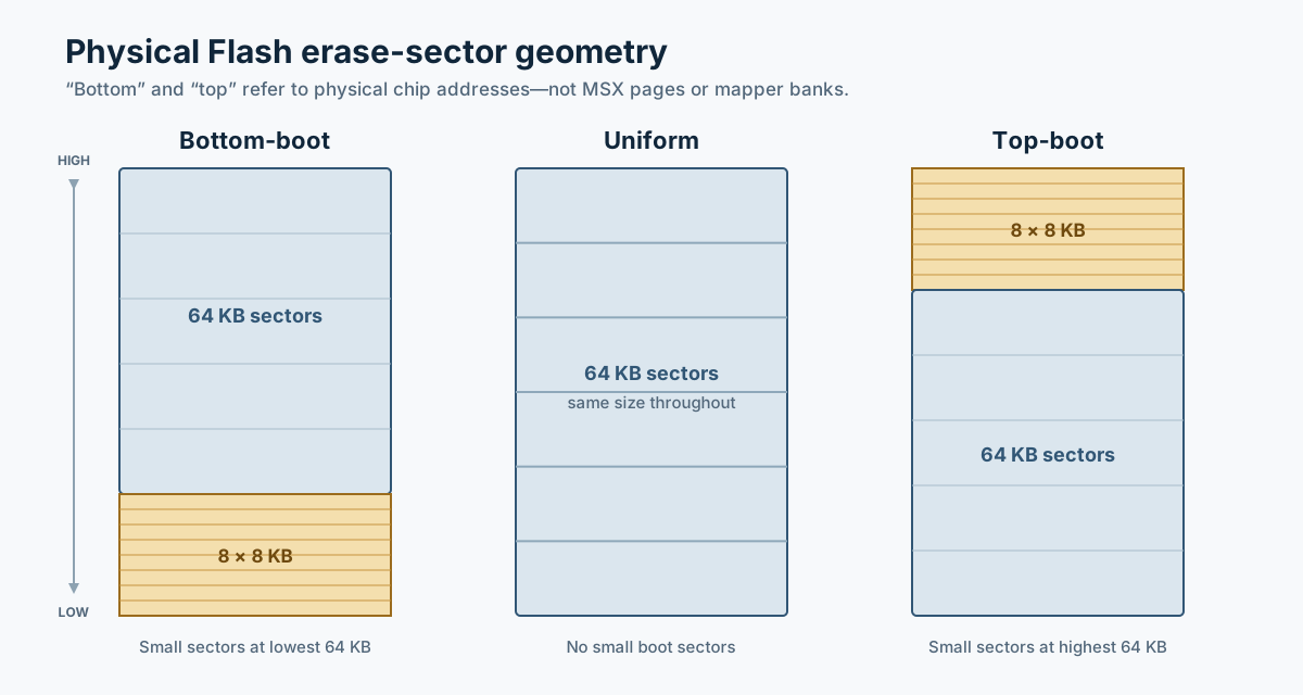
The letters in a Flash part number often identify the geometry. For example, the Micron/Numonyx M29W640GB is the bottom-boot version and the M29W640GT is the top-boot version; uniform variants use 64 KB sectors throughout. The ASCII16-X specification describes the common bottom-boot arrangement used by its reference cartridge: the first eight sectors are 8 KB and the remaining sectors are 64 KB.
If your program genuinely needs to discover the installed device, use the chip’s CFI query and decode the erase-region descriptors. If maximum compatibility is more important than using every last byte, the simpler rule is to reserve ordinary 64 KB sectors and avoid making the save format depend on any 8 KB boot-sector arrangement.
Why the physical bottom of a multifunction cartridge is usually not game space
On a simple cartridge containing only one ROM, physical Flash address zero may also be the beginning of that ROM. On a multifunction or multi-ROM cartridge, that assumption is unsafe. The cartridge needs its own firmware, directory records, BIOS images, recovery data, or ROM-disk data somewhere in Flash.
Carnivore2 documents this precisely. Its first physical 64 KB is the eight-sector bottom-boot area and contains Boot Menu code, directory entries, and Boot Menu data. The following 64 KB blocks contain the IDE BIOS and FMPAC BIOS; ordinary ROM-image storage begins later. Those are cartridge-owned regions, not spare sectors for a game. See the Carnivore2 technical description for the physical block map.
MegaFlashROM SCC+ SD also keeps cartridge-managed components in Flash, including the SD kernel, disk ROM, optional ROM disk, and recovery program. OPFXSD manages those areas and the placement of loaded ROMs. A game should therefore treat its mapped ROM image as its address space and should not assume that physical chip offset 000000h belongs to it.
Multiple ROMs: the physical location can move while the logical location stays the same
A game normally addresses Flash relative to its own ROM image: logical bank 0, logical bank 1, and so on. The cartridge loader chooses a physical image base in the Flash chip and configures the mapper so those logical banks reach the correct physical blocks.
If more ROMs are installed, deleted, or reorganized, the same game image may begin at a different physical Flash block. Its internal layout does not change. A save sector reserved at a fixed logical offset near the end of the ROM remains at that same offset inside the image; only its absolute chip address changes.
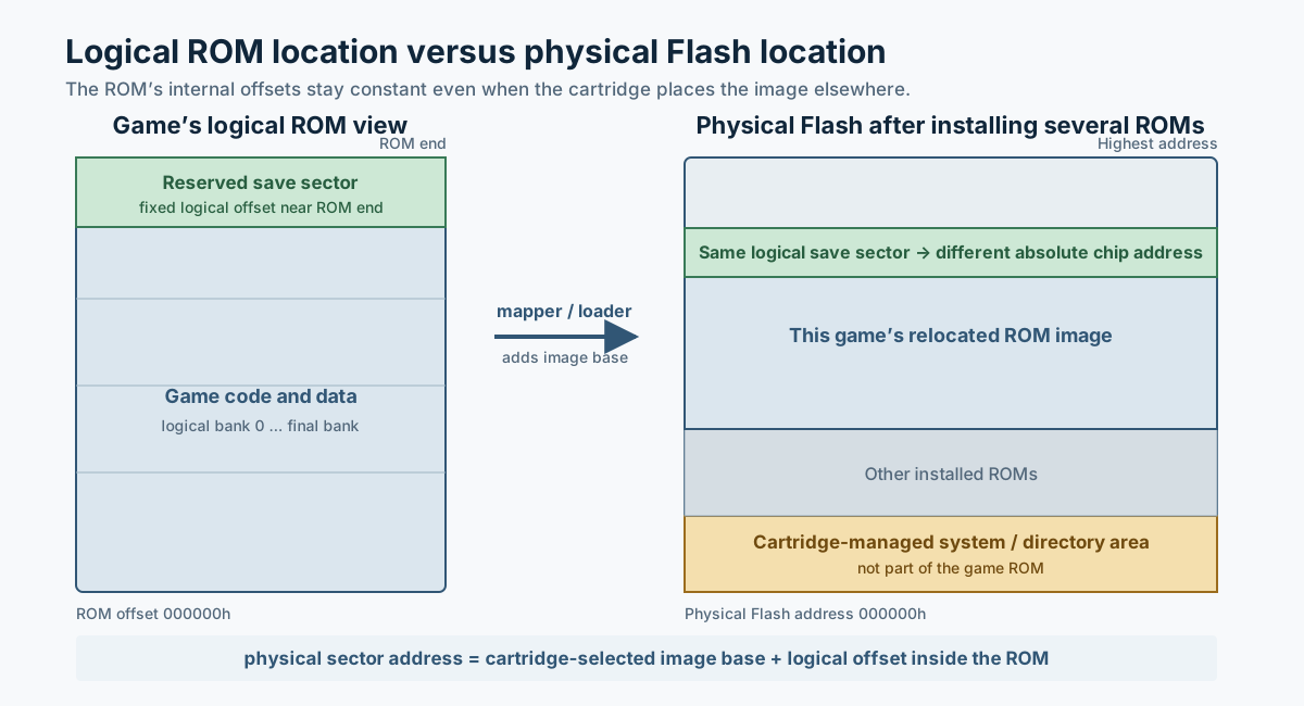
physical Flash address = cartridge-selected image base
                       + logical offset inside the ROM image
This relocation only works safely when the cartridge configuration maps writes to the same Flash image that it maps for reads. MegaFlashROM must launch the title in its self-writing mode, and Carnivore2 must use an RCP whose relevant bank engines permit writes. The ROM should reserve its save sectors as part of the ROM image so the loader moves the game and its save area together.
8. One address space, four MSX pages — how all cartridges fit together
Before looking at MegaFlashROM, Carnivore2 or ASCII16-X, it helps to separate three different ideas that are often mixed together: the MSX CPU page, the ROM mapper bank, and the physical FlashROM sector. They are related, but they are not the same thing.
The MSX standard: four 16 KB CPU pages
The Z80 has a 64 KB address space. MSX divides that address space into four standard 16 KB pages:
| MSX name | Z80 address range | Meaning |
|---|---|---|
| MSX Page 0 | 0000h–3FFFh | First 16 KB of the CPU address space |
| MSX Page 1 | 4000h–7FFFh | Normal lower cartridge ROM window |
| MSX Page 2 | 8000h–BFFFh | Normal upper cartridge ROM window |
| MSX Page 3 | C000h–FFFFh | Normally system/game RAM |
These names should be our primary terminology throughout this article. “Page 1” always means 4000h–7FFFh, regardless of which cartridge is being used. The MSX slot hardware also selects which slot is visible independently in each of these four pages.
Where an ASCII16 game normally lives
A conventional ASCII16 cartridge uses the middle 32 KB of the Z80 address space: MSX Page 1 (4000h–7FFFh) and MSX Page 2 (8000h–BFFFh). Mapper writes select which 16 KB portions of a larger ROM appear in those two CPU pages.
That is why Flash-saving code for an ASCII16-style game will normally issue its Flash commands and data writes through addresses in Page 1 and/or Page 2. The physical save sector may be near the end of a multi-megabyte FlashROM, but the CPU still reaches that sector through one of these 16 KB windows after mapping the appropriate ROM bank.
Flash writing adds another layer
The Flash chip does not care that the programmer calls an address “MSX Page 1” or “MSX Page 2.” It sees the physical Flash address produced by the cartridge mapper. To program or erase Flash, every write in the command sequence must actually reach the Flash chip: the unlock writes, command writes, and final data or sector-confirm write.
This gives us a useful mental model:
Z80 address
    ↓
MSX Page 0 / 1 / 2 / 3
    ↓
cartridge mapper window
    ↓
selected ROM/Flash bank
    ↓
physical Flash address / erase sector
For example, a game may map a save area located near the end of a 4 MB ROM into 8000h–BFFFh. The CPU is writing through MSX Page 2, even though the physical Flash address is several megabytes from the beginning of the chip.
How the three cartridge solutions differ
| MegaFlashROM SCC+ SD | Carnivore2 | ASCII16-X | |
|---|---|---|---|
| MSX CPU pages | Still the standard MSX Page 0–3 address ranges. | Still the standard MSX Page 0–3 address ranges. | Still the standard MSX Page 0–3 address ranges. |
| Typical ASCII16 game access | Page 1 4000h–7FFFh and Page 2 8000h–BFFFh. | Page 1 and Page 2 for the standard ASCII16 RCP. | Page 1 and Page 2. |
| Extra permission before self-writing | The ROM must be installed in a write-capable configuration; for OPFXSD this is the reason for using the appropriate /W setup for a self-writing title. | Write permission is controlled per Carnivore2 bank by bit 4 of RnMult. The RCP decides which banks—and therefore which CPU windows—accept writes. | No Carnivore2 RCP layer. The ASCII16-X mapper/Flash implementation directly provides the Flash behavior expected by the ROM. |
| Flash protocol | The game can use the same compatible AMD/JEDEC-style program/erase command logic when the underlying Flash implementation supports it. The cartridge-specific job is making sure those writes actually reach the intended Flash bank. | ||
Carnivore2 terminology: MSX Page is not Carnivore2 Bank
This is the easiest place to get confused. Carnivore2 has four configurable hardware Banks 1–4. Those numbers do not mean MSX Pages 0–3. Each Carnivore2 bank has a BnAdrD value that specifies where that bank appears in the Z80 address space.
For the standard Carnivore2 ASCII16 configuration the relationship is:
| MSX standard terminology | CPU range | Carnivore2 ASCII16 terminology |
|---|---|---|
| MSX Page 0 | 0000h–3FFFh | Carnivore2 Bank 4 |
| MSX Page 1 | 4000h–7FFFh | Carnivore2 Bank 1 |
| MSX Page 2 | 8000h–BFFFh | Carnivore2 Bank 2 |
| MSX Page 3 | C000h–FFFFh | Carnivore2 Bank 3 |
0000h–3FFFh, which is MSX Page 0. The mapping can be different in another RCP because BnAdrD is configurable.
Our RCP utility therefore shows both names. It should say, for example, “MSX Page 1 — 4000h–7FFFh — Carnivore2 Bank 1”, rather than presenting “Bank 1” by itself. When an existing RCP is dropped into the utility, the displayed MSX address range is decoded from that RCP instead of assuming the standard ASCII16 arrangement.
What should normally be writable?
For a typical ASCII16/ASCII16-X game, start with MSX Page 1 (4000h–7FFFh) and MSX Page 2 (8000h–BFFFh), because those are the normal cartridge ROM windows. On the standard Carnivore2 ASCII16 RCP these are Carnivore2 Banks 1 and 2.
But do not turn on pages mechanically. Look at the addresses used by the actual Flash routine. If any unlock, command, program or erase-confirm write goes through another CPU window, the Carnivore2 bank covering that window must also permit writes. Conversely, if a page is never used for Flash writes, leaving it protected is preferable.
This also explains why the same game-side Flash routine can be made to work across MegaFlashROM, Carnivore2 and ASCII16-X. The MSX-side addresses and Flash command protocol can remain the same; what changes is how each cartridge maps those addresses to Flash and whether it permits the writes.
9. MegaFlashROM SCC+ SD
MegaFlashROM adds a very important extra requirement: a ROM can be launched with its Flash area effectively read-only.
/W option.
OPFXSD GAME.ROM /WAccording to information provided by Manuel Pazos, OPFXSD normally makes the launched ROM read-only. The /W parameter is required when the running ROM needs to program its own FlashROM area. OPFXSD can also recognize specific ROM checksums and automatically apply the equivalent write-enabled setup for known titles.
For a released game, it is therefore useful to document the required /W parameter prominently. It may also be possible to have the title recognized by OPFXSD so users do not need to remember the option manually.
10. Carnivore2: choose exactly where Flash writes are allowed
Carnivore2 has four independently configurable mapper banks. Each bank has an RnMult byte, and bit 4 controls whether CPU writes are passed to that bank: 0 = protected, 1 = writable.
The bank number itself does not permanently mean a fixed Z80 page. BnAdrD selects where the bank appears in the CPU address space, while the low three bits of RnMult select its size. Therefore an RCP editor must decode the actual CPU window instead of assuming R1/R2/R3/R4 always mean 0000h/4000h/8000h/C000h.
For a normal ASCII16 ROM
The documented Carnivore2 ASCII16 preset places its four 16 KB banks as follows:
| C2 bank | Z80 CPU window | Recommended write setting |
|---|---|---|
| Bank 1 | 4000h–7FFFh | Usually enable |
| Bank 2 | 8000h–BFFFh | Usually enable |
| Bank 3 | C000h–FFFFh | Normally protect |
| Bank 4 | 0000h–3FFFh | Normally protect |
4000h–7FFFh and 8000h–BFFFh is the sensible default. These are the normal cartridge ROM windows. But this is a convention, not a Carnivore2 hardware limitation.Why you may need more than the page containing the save data
The complete Flash command sequence has to reach the Flash chip. That includes the unlock writes, command writes, and the final program-data or sector-erase confirmation write. If part of your command sequence goes through 4000h–7FFFh and another part goes through 8000h–BFFFh, both windows must be writable.
You can also deliberately use Flash through 0000h–3FFFh or C000h–FFFFh. In that case enable the corresponding bank too. The safest rule is simple: enable writes only for every CPU window your Flash routine actually writes through, and leave the rest protected.
What changes inside an RCP
The RCP contains six bytes for each bank: RnMask, RnAddr, RnReg, RnMult, BnMaskR, and BnAdrD. To enable writes without disturbing the mapper setup, set only bit 4:
RnMult = RnMult OR 10h      ; enable writes
RnMult = RnMult AND EFh     ; disable writes
For an existing RCP this matters: the other RnMult bits control whether the bank is active, Flash/RAM selection, mirroring and bank size. They must be preserved.
Embedded Carnivore2 RCP editor / generator
Drop an existing .RCP to edit it. If you do not load a file, choose a mapper and create a new one from the documented Carnivore2 defaults. Imported files are kept intact; the tool changes only the four RnMult write-enable bits.
or click to choose a file. Leave empty to create a new RCP.
Advanced: decoded bank bytes
Imported files preserve every original byte, including bytes beyond the documented 30-byte RCP structure. Only offsets 04h, 0Ah, 10h and 16h are changed by these write-enable controls.
Official RCP layout: byte 00h = mapper character; bank records occupy 01h–18h; R1Mult/R2Mult/R3Mult/R4Mult are at 04h/0Ah/10h/16h; 19h–1Ch contain Mconf, CardMDR, PosSiz and RstRun; 1Dh is reserved and normally FFh.
11. ASCII16-X and openMSX
ASCII16-X was designed with direct Flash programming in mind. There is no OPFXSD-style launch option required for the cartridge itself. The game still needs to map the correct Flash banks, execute the Flash routine from RAM, and target a valid sector.
One ASCII16-X-specific detail is that mapper registers are also visible in bank 2. For Flash command/data writes you should avoid addresses in B000h–BFFFh; use the equivalent locations through the appropriate 7000h–7FFFh mapping instead.
openMSX
When testing, make absolutely sure the ROM is configured as ASCII16X, not ordinary ASCII16. A recent real-world debugging case looked exactly like a failed Flash command sequence: the debugger kept returning normal ROM data because the launch script had accidentally hardcoded the normal ASCII16 mapper. Once changed to ASCII16-X, the same programming code worked as expected.
Modern openMSX versions emulate the ASCII16-X Flash behavior and timing, making them useful for testing the exact same DQ7/DQ5 logic used on hardware. Final testing on real cartridges is still recommended.
12. A practical cross-cartridge save design
A robust arrangement is to reserve two ordinary 64 KB sectors near the end of the ROM and alternate between them.
- Keep the currently valid save in sector A.
- Leave sector B erased and ready.
- When an update eventually requires 0 → 1 transitions, write the new complete save image into sector B.
- Verify the new data.
- Only after verification, treat sector B as current.
- Erase old sector A so it is ready for the next update.
- Swap the roles next time.
For small state changes such as achievements, flags or counters, you can often avoid an erase altogether by using fresh 1-bits and only programming 1 → 0. A log-style format can append new records until a sector fills, then compact into the alternate sector.
For maximum cartridge compatibility, do not make your save format depend on the first chip-specific 8 KB sectors just to save space. A 64 KB reservation is inexpensive in a multi-megabyte ROM and substantially simplifies hardware compatibility.
13. Troubleshooting checklist
| Symptom | Check |
|---|---|
| Writes appear to do nothing on MegaFlashROM | Was the ROM programmed/launched with OPFXSD /W? |
| Writes appear to do nothing on Carnivore2 | Does the ROM's Carnivore2 configuration have the relevant bank's write-enable bit set? |
| Works on hardware but not openMSX | Verify the mapper is ASCII16X, not ASCII16. Use a recent openMSX version. |
Polling immediately sees FFh | The command may not have been accepted. Check mapper/bank setup, unlock addresses and write protection. |
| DQ5 error when programming | Check whether the requested new byte attempts any 0 → 1 transition. If so, erase the sector first. |
| Code crashes during erase/program | Make sure the actual Flash writer and polling routines execute from RAM. |
| Works on one Flash cart but not another | Check sector geometry. Avoid assumptions about 8 KB boot sectors; use ordinary 64 KB sectors. |
| Wrong sector erased | Verify which physical Flash bank is mapped at the MSX address receiving the final 30h. |
References and further reading
- MSX Resource Center: ASCII-X FlashROM cartridge discussion — includes the original working routines and subsequent explanations/debugging.
- ASCII16-X specification — mapper and FlashROM documentation.
- M29W640G Flash datasheet — bottom-boot, top-boot and uniform erase-sector maps.
- MegaFlashROM SCC+ SD user manual — OPFXSD, SD kernel, disk ROM, ROM disk and recovery installation.
- Carnivore2 technical specification — Flash layout and mapper configuration registers.
- Carnivore2 user guide — ROM loading, configuration presets and cartridge management.
Article assembled from the public ASCII-X development discussion, the tested Max Iwamoto Flash routines, explanations by Max Iwamoto and Laurens Holst (Grauw), MegaFlashROM information from Manuel Pazos, and public Carnivore2 technical documentation. Flash programming always carries a risk of corrupting data if the wrong bank or sector is selected; test with disposable ROM images/hardware configurations first.